Producing nanocircuits with graphene fluoride
KTH Theoretical Chemistry researchers, along with colleagues at the University of Technology and Science in China, have been developing a new method of producing nanoscale electronic circuits that may allow us to produce even faster computers.
by Yi Luo,
KTH Department of Theoretical Chemistry
Imagine a sheet of carbon that is just one molecule thick! That is graphene - the thinnest and strongest form of carbon. It is a hundred times stronger than steel, conducts heat better than any other known material, and conducts electricity just as well as copper does. Now add a fluorine atom to each of the carbon atoms and you get graphene fluoride or fluorographene, which is stronger and more chemically stable than graphene. Fluorographene however has lower electrical conductivity, and so it is classed as an insulator.
Thanks to these properties, fluorographene has been investigated for use in very, very small electronic circuits, known as nanocircuits – tiny electrical circuits with measurements in the millionths of a millimetre. As you can imagine, we cannot build circuits on such a small scale by hand, so special techniques are necessary to construct these incredibly small circuits. As fluorographene is such a thin substance, it is potentially useful in nanocircuits where it could be used as an extremely thin insulator to separate conducting graphene channels from each other and thus form a minuscule electronic circuit.
Fluorographene nanocircuits are potentially vital in supercomputers, as the speed of our computers is determined by the number of field-effect transistors on each of the computational chips in the computer. To put more transistors into a computer chip, we need to decrease the size of them, and that is where these tiny graphene-based nanoscale electronic circuits could be used.
The development of the first graphene-based field-effect transistor was reported in 2007, however that transistor could not be switched off because of its large conductive graphene area, which made it unsuitable for realistic applications. In 2012, Yi Luo’s research group at the Department of Theoretical Chemistry, KTH Royal Institute of Technology, together with their experimental collaborator, Prof. Xiaoping Wang from the University of Science and Technology of China (USTC), proposed using catalytic scanning probe lithography (cSPL) to directly write electronic devices on graphene oxide (which is the single layer form of graphene with oxygen, rather than fluorine, added to it).
In the cSPL technique, a microscopic or nanoscopic stylus bearing a catalyst is moved mechanically across a surface to form a pattern, which results from the interaction of the catalyst with the surface. Using these probes to directly catalyse a variety of localised chemical reactions makes it possible to generate nanoscale features with a high degree of chemical complexity in a “direct-write” manner, almost as if one were printing the resulting chemical substance onto the surface.
Graphene oxide has been considered as a possible means of producing graphene nanocircuits, however there have been problems with producing graphene oxide of a suitable quality. In comparison, fluorographene can be readily obtained by exposing graphene under xenon difluoride gas, making it a better material for practical applications. Therefore, it is worth considering using the new cSPL method to partially reduce fluorographene (rather than graphene oxide) in order to build nanocircuits. Xinrui Cao, Yongfei Ji, Wei Hu and Sai Duan from Yi Luo’s research group at the KTH Department of Theoretical Chemistry have been using Lindgren to investigate ways to do just that. With the help of high accuracy first principle simulations, they have proposed a new strategy for fabricating nanoscale electronic circuits on graphene fluoride using the cSPL technique.
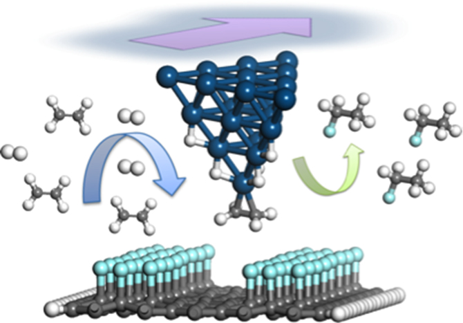
The scheme that the KTH researchers have proposed uses the cSPL “direct writing” technique to “write” electronic circuits onto fluorographene at a low temperature compared to that which would be needed for graphene oxide – this is a promising method for practically producing nanocircuits. Their research is mainly focused on simulating these processes using first principles and using the resulting information to design suitable molecular electronic devices for production. It is very important to simulate the production method first because the results obtained from the theoretical simulations make it possible to avoid damage to the equipment and instruments, as well as to operators, when it comes to performing the experiments. For example, simulation results indicate that the tip-induced reduction of fluorographene in a hydrogen atmosphere would release the hazardous gas, hydrogen fluoride. Consequently, when practical experiments are started, the researchers would definitely not perform the experiments in an atmosphere of hydrogen.
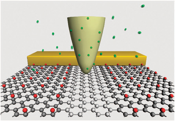
In one particularly interesting simulation project that was run at PDC, Yi Luo’s group studied the possibility of directly writing nano-electronic devices on a single layer of graphene fluoride with the tip of an atomic force microscope that is coated in platinum. The diagram on the opposite page shows how the graphene fluoride is chemically reduced (that is, how it gains additional electrons) with the cSPL technique using a mixture of hydrogen and ethylene. The reduction reaction removes some parts of the fluorine when scanning the fluorographene surface with the platinum-coated tip. This changes the fluorographene in those areas to graphene and thus a conductive graphene channel is created on the surface. Using this method nanocircuits can be built without using or producing any hazardous products.